Get a Quick Online Quote: Register or Login

Seamless PCB Manufacturing Checklist

When preparing for the fabrication of a printed circuit board (PCB), a lot of things have to be planned carefully in the right way.

If one step or consideration is overlooked, it may have disastrous consequences resulting in a malfunctioning board. Our seamless PCB manufacturing checklist will help you ensure every part of the circuit board is considered and potential mistakes practically eliminated.

Seamless Manufacturing Checklist

This checklist is how we process our PCB orders from start to finish for our customers.

Fill out the checklist below, download it, print it, and/or submit it to us to get started on a quote.

Be sure to go down the list and make sure all of these are checked to save yourself from all of the painful mistakes and headaches when you realize you’ve got something missing.

Checklist Item Criteria Yes No
1) MATERIAL: Do you have your material type (FR4 or other) determined?
Cu Weight Internal Layers: Do your Cu weight internal layers fall within 1/2 oz - 2 oz & line/space ≥.003 - Min. line/space ≥.006?
Cu Weight External Layers: Do your Cu weight external layers fall within 1/2 oz - 2 oz & line/space ≥.003 - Min. line/space ≥.006?
2) PLATING: Are holes and conductive surfaces plated per IPC-6012 Class II?
3) SOLDERMASK: Is solder mask required? For example: component side only, solder side only or both sides & color.
4) FINISH: Do you know which surface finish to use? For example: ENIG, HASL, Silver, ENEPIG, etc.
5) SILKSCREEN: Is silk screen required? For example: component side only, solder side only or both sides & color.
6) LOGOS & DATE CODE: Is the vendor UL logo & date code required?
7) TOLERANCES: Do you know what tolerances you will be using (finished hole tolerance ±3 mils, linear tolerance ±10 mils, or PCB thickness tolerance 10% ≥ 3 mils)?
8) FABRICATION & ACCEPTANCE GUIDELINES: Will you be requiring fabrication and acceptance guidelines that fall within IPC-6012 Class 2?
9) FILES: Are you able to supply manufacturing files? Example: drill/gerbers or ODB++.
10) FABRICATION SPECS: Do you have a fabrication drawing with specifications, tolerances, etc.?
11) FIDUCIALS: Do you have local fiducials for assembly?
12) ASSEMBLY: Do you have a BOM (bill of materials with part #s and notes), pick and place file (X & Y coordinates of the components), and an assembly drawing with reference designators, pin 1 locations, anode/cathode locations?
13) ASSEMBLY TYPE: Do you know what type of assembly this will be? (RoHS/leaded or clean/no clean)

Are you sure?

Examples for Reference

Fabrication Drawing Example

Fabrication Drawing Example

Here's an example of an assembly drawing: Fab Drawing Example.pdf

Bill of Materials (BOM) Example

Bill of Materials (BOM) Example

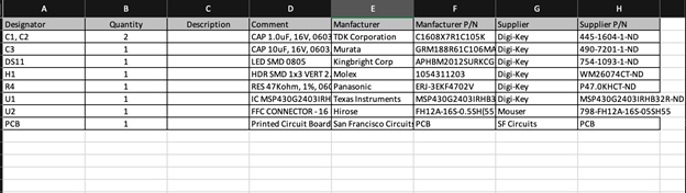
Here's an example of a Bill of Materials for PCB Manufacturing: Example BOM

Ready to Process Your PCB Order?

Now that you have your manufacturing checklist, you’ll know exactly what you need to have a seamless manufacturing process. If you’re ready to get a quote, you have all that you need to get an accurate estimation on placing your order. You can refer to this checklist while you place a quote through our website.

At SFC, our specialty is advanced PCB fabrication and assembly producing excellent multi-layered PCBs and unparalleled technical expertise at competitive prices. Many of our customers request PCB production with higher expectations compared to other normal circuit board providers.

Are you looking for PCB fabrication or PCB assembly? We’ve got you covered. We hope the notes and manufacturing checklist above are helpful for you. From intricate concepts to more standard designs, we welcome the challenge and will bring your ideas and designs into reality.

From PCB manufacturing to PCBA, we can do it all!

Get a Quote: 1-800-SFC-5143

Or EMAIL US to discuss & quote your project

San Francisco Circuits, Inc.

1660 S Amphlett Blvd #200
San Mateo,CA 94402
Toll-Free: (800)732-5143
E-mail: sales@sfcircuits.com

 NIST LogoITAR Compliance Seal  IPC International, Inc. Membership Seal SAM

San Francisco Circuits - San Diego

3914 Murphy Canyon Rd., Suite A244
San Diego, CA 92123
Local: (858)576-7202

Follow us

Twitter Logo Facebook Logo LinkedIn Logo

©Copyright 2005 - 2024 - San Francisco Circuits, Inc. - All rights reserved

Latest News

02-21-2024

Via tenting is the application of soldermask to encase or seal the via’s opening. A via is essentially a hole drilled into the PCB that facilitates connections between multiple PCB layers. An untented via, on the other hand, remains uncovered by a soldermask layer. The decision to expose or cover these vias carries both advantages and disadvantages contingent upon your specific design and manufacturing requirements.

Read more

11-30-2023

The Essential Guide to PCB Assembly Drawings: Understanding Polarities, Pin1 Marking & Anode/Cathode Markings. Learn more about understanding the XY File, component locations, & polarized component orientations.

Read more

User Login