Wearable technology has made great strides in recent years. The materials and innovation in this sector are constantly progressing from research and development teams to meet the extreme design requirements of size, heat dissipation, power absorption, flexibility, and weight.
From fitness wearables for consumers and everyday use to high-level medical sensors, one constant is found in modern wearables - a need for small form factors.
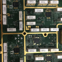
Small form factors, or miniaturization, in more cases than not, are achieved through the use of multi-layered (typically 2 to 8 layers) flex PCBs for these wearable devices.
Flexibility: Bending & Flexing in Small Form Factors
Flexible circuit boards offer flexing and bending ability, perfect to form to the unique contours of the wearer’s body. They also dynamically flex, meaning they stay connected throughout the movements and environmental changes common in wearable devices. The polyimide material they are made of can also withstand the constant impacts, shocks, and vibrations of human movement.
Wearable flex PCBs also minimize failure points that commonly occur with traditional rigid PCBs at interconnect points, like poor solder joints. With flex materials, the interconnect points are removed or simplified.
Weight, Comfort, & Safety
Movement and flexibility are important wearable device attributes, but neither would be possible without practicality. Wearable devices need to be comfortable and, therefore, as lightweight as possible. Naturally, these are also important attributes that flex materials have over rigid FR4 materials.
The flexible polyimide has also been approved by the FDA to be in contact with human skin and not known to cause any allergic reactions.
Heat mitigation is also important for comfort. These devices cannot generate a lot of heat so they remain comfortable for the wearer.
Communication
Of course, most wearable technologies will also feature some form of communication with another device or larger system so wireless, high-speed RF PCB, and/or Bluetooth technologies are critical and important components of these devices.
Versatility & Environmental Resistance
Like the wearers, many devices may find themselves exposed to the elements - extreme cold, heat, water resistance, and water submersion resistance.
Material selection, therefore, is critical to ensure the success and long term usage of the device:
Moisture considerations are especially important for electronic circuits that are of high impedance. The designer must consider whether the device is hermetically sealed or a solution where the PCB is treated with a conformal coating to protect it. Whatever solution is used, insulation of the components is also critical to protect the user’s skin from electronic dispersion.
.png)
We can turn your rigid flex PCBs in 7 days with .006" min hole size & .003" min. trace/space.
For applications that require high-frequency / high-speed signals, materials with lower dielectric constants (Dk) will typically be utilized.
Polyimide films are the flex material of choice for most wearable applications. P95 from Isola Group is an ideal choice with a low Dk of 3.76 (compared to FR4 Dk of ~4.5).
Dissipation factor (Df) also needs to be considered when selecting the material for wearables. A low Df will mean less signal strength lost when passing through components, systems, and materials. The aforementioned P95 material boasts a Df of .017 at 2.5 GHz.
Coefficient of thermal expansion (CTE) and high Tg are also important to check on the material as these tiny, crowded PCBs will need strong stability throughout extreme temperature ranges.
Optimizing the design of a wearable PCB is critical as the wearable device will typically require a small form factor, light weight, minimal presence, environmental protection, heat mitigation, durability, and flexibility.
Wearables using a rigid flex PCB must consider the interconnect points, in addition to impedance control. At high frequencies, small impedance mismatches can create big signal distortions and communication issues, so impedance matching your circuit will be critical to reducing signal loss. Bends in the rigid flex must also be precise to perfectly line up and not put stress on the connection points, increasing the potential of failure. Utilizing a flex-only approach will mitigate the risks that come with rigid flex and these interconnect points.
Read more on PCB Interconnect Design
The designer should consider some best practices for their wearable device PCB layout:
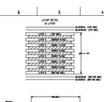
Some of these considerations will, in turn, impact the number of layers used in the stackup. A higher layer PCB (6 or 8 layers for example) can be advantageous for the ground and power planes to be contained between components and lines.
| Specifications | Standard Technology | Advanced Technology |
|---|---|---|
| Number of Layers |
1 - 12 |
14 - 40 |
| Quick Turn Times |
up to 24 hours for bare board fabrication or assembly (1-6 layers) |
|
| Minimum Board Thickness |
2 layer - 0.010" 4 layer - 0.020" 6 layer - 0.020" 8 layer - 0.062" 10 layer - 0.062" 12 layer - 0.062" |
2 layer - 0.005" 4 layer - 0.010" 6 layer - 0.031" 8 layer - 0.040" |
| Maximum Board Thickness |
2 layer - 0.125" 3-12 layer - 0.200" |
0.250" - 0.500" |
| Maximum Board Size |
16" x 22" 12" x 21"
|
10" x 16" 16" x 22" 12" x 21"
|
| Copper Thickness |
0.5 oz - 3 oz |
4 oz - 10 oz |
| Hole Aspect Ratio |
7 : 1 |
15 : 1 |
| Minimum Hole Size |
0.008" |
0.004" |
| Minimum Trace/Space |
0.006"/0.006" |
0.002"/0.002" |
|
Minimum Drill-to-Copper |
0.010" |
0.005" |
| Minimum Pitch |
1 mm |
0.3 mm |
| Final Finish |
HASL (Solder) Lead Free Solder Copper Gold Gold Fingers White Tin ENEPIG ENIG |
HASL Gold (ENIG/Hard/Soft) Selective Gold Immersion Silver OSP White Tin ENEPIG |
| Additional Features |
Plated Slots Non-plated Slots Controlled Dielectric Covered Vias Counter Sinks Counter Bores Dual Access Flex Suspended Leads |
Plated Edges Plated Milling Plated Counter Bores & Counter Sinks Edge Castellation Controlled Impedance Silver Filled Vias Non-Conductive Filled Vias
|
| Quality Standards |
IPC 6012 Class 2 Electrical Testing 100% Netlist Testing TDR Testing |
Milspec 31032 Milspec 55110 Milspec 50884 IPC 6012 Class 3 100% Netlist Testing TDR Testing |
| Special Technology |
|
Blind & Buried Vias Laser Drilled Vias Mechanically Drilled Micro Vias |
Source, Northwestern Mccormick School Engineering
The future of materials for wearable technologies is certainly exciting and sure to evolve.
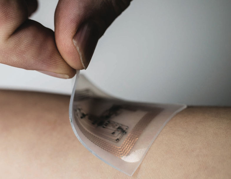
Wearable skin-line devices are being researched. One notable researcher is John Rogers of Northwestern who has developed a suite of health monitoring devices that look and feel like temporary tattoos, softly adhering to the surface of the skin. Rogers’ institute also develops new materials that can be implanted into the person and monitor vitals.
Biomaterials are also a possibility with biocompatible based substrates made of protein films.
Connected clothing wearables, or e-textiles, have been in development at the University of Bayreuth with textiles capable of conducting electricity via tiny silver wires 80 nanometers in diameter.
Devices that power themselves via sunlight, heat, or motion could be further developments in the wearable technology space that are being tested at places like Finland’s University of Oulu.
With these advances come advancements in IPC standards for these types of new materials, devices, and requirements.
Overall, with more stringent demands on wearable placement and biocompatibility, advances in sensor capabilities, component miniaturization, and battery efficacy, we’re sure to see great strides in materials and solutions in years to come.