They say that timing is everything. When it comes to signal integrity in a digital system, “they” are not far off. Even in an analog system, the prevailing wisdom is that shorter is better. Both disciplines make use of trace length as a means of increasing performance. On the digital side, we’re concerned with keeping numerous signals in sync with a clock while analog networks have their own quirky reasons for using delay lines.

Beautiful intricate PCB board design. Source: Autodesk
Let’s start off with the digital domain. We like to imagine a marching band that moves and plays in lock step to the beat of the drum line. The big bass drum ticks off the down beat–known as the “one”. Everything starts with the one. Snare drummers add their flavor on the back beat and provide fills. With that, you have the one and then the zero. Horn players and everyone else alternately play and rest over those two events to bring out the melody. There, you have the data.
The drum core is the clocking element of the band. The rhythm section lays down a groove for the melody. On a printed circuit board, that timing duty is, of course, the net or nets with “CLK” in their name. Note that CLK is the usual signifier of a clock net when used in the schematic. The clock never takes time off. Meanwhile, the other members of the bus get to have periods when they are at rest.
The fact that the clock is switching continuously while the others are intermittent is why the clock is the noisy one. The switching rate is determined by the controller chip or an external oscillator. The little collection of capacitors and/or resistors around the crystal along with careful routing are part of the effort to get a clear pulse for all that follows.

Figure 1. An internal layer revealed to show length matching schemes.
When we talk about double-data-rate (DDR) it’s not the clock but the other signals that act on the downbeat and the backbeat. That would make you think that those would be twice as noisy as the clock, and they would be if it weren’t for all of those rest periods. We pay strict attention to the threshold of when those DDR signals pass from a low voltage state to a high voltage.
Note that “low” generally means zero volts and high can be anything from one volt to five volts. It’s all low voltage relatively speaking. It doesn’t go much higher because higher voltage swings create more noise. We like to run our crystals on 1.8 volts while the rest of the circuitry is switching between zero and 3.3 volts.
The power tree of a complete system might start off with 110/220VAC from the wall socket and step it down while converting to direct current using a power supply circuit. The circuit can be a collection of parts placed and routed on the board using a transformer, inductors, capacitors, resistors and diodes.
The transformer reduces or increases the voltage depending on how many windings are on either side. The inductors and caps smooth out the flow while the resistors are used to divide the power into various smaller voltages. Finally, the diodes keep the current typically flowing in one direction. Power supply modules are popular because they take the risk out of designing all of this to pass UL and FCC regulations. Underwriters Laboratories (UL) is the group who certifies that your product won’t easily catch on fire while the Federal Communications Commission (FCC) ensures that it will play well with other electronics. Both of those are necessary approvals for commerce.
Mobile devices will take battery or “wall wart” power which are already direct current and split the VBAT or VIN into 1.2, 1.8, 2.5, 3.3, 5.0, and maybe 9 or 12VDC. It’s all going to depend on the component mix. Even if every part uses the same voltage potential, they tend to want their own isolated version of that rail.
Low voltage switches faster because it’s a lower amplitude of change. Low voltage is also more susceptible to picking up enough noise to make it difficult to decide if the signal is supposed to represent a high or low state. Millivolts add up quickly when the whole range is one volt. It’s like the brass has to take a breather so that we can hear from the woodwinds and the flutes.

Single ended or differential, traces use serpentine to meet timing budgets.
So, where were we? Ah, yes, busses of all kinds, each different type running around on one of many possible voltage swings. Low voltage signals need their space so they don’t get muddied up by the higher voltage devices.
Data packets are sent down the line(s) and followed by a pause when the transmitting device sends a quick stream of ones and zeros that represent the total number of bytes that were transmitted. The number of bits in a byte and other frameworks such as whether there is a stop bit, parity, and duplexing are all established by the firmware.
In this way, the receiver end knows this burst of data with the number of bytes is coming and counts up the number of bytes that it received. If the number transmitted matches the number received, then the receiver keeps listening for more. If the “checksum” is different, the receiver says, “hold up, send that last packet again.”
Dropped packets are bad news because they slow the system down. Even if sending the redundant data doesn’t affect the operation of the actual program, it still eats up clock cycles. Every clock cycle uses a tiny fraction of energy and makes a little pulse of noise. Unnecessary use of energy and generation of noise makes a system that much more inefficient. Proper timing of the signals lowers the bit-error-rate (BER) so the whole system runs better.
Taken in isolation, signal integrity relies on two main factors, timing and impedance.
Timing is a function of length but not in a strict sense. Time of flight from the junction of one piece of silicon to another considers the entire path. Gold or aluminum wire bonds have a certain propagation velocity. Ceramic materials used on substrates create less delay than typical FR4 materials used on the PCB. Signals propagate faster on outer layers or even faster though the air. Overall length works against you since the traces always have resistance, capacitance. and inductance.
For example, a wireless transmitter may have a setting for mimicking different lengths of guitar cable. The idea is to compensate for the amount of high frequency attenuation caused by each foot of wire. On bass, it doesn’t matter that much but some guitarists consider the cable as part of their tone. High speed digital is more like the guitar player.

Figure 2. Strapped to the bottom of the guitar pedal board, the wireless receiver has a variable low-pass filter to simulate using a typical length of cable.
The high frequency part of the signal is where the data lives. Other low-frequency signals with higher amplitude have a tendency to create harmonics of their fundamental frequency. Those spurious signals are the ones that will latch on to the high frequency signals of the bus. In that way, a one megahertz signal can destroy a 2.5 Ghz signal. Spacing alone is not enough when there is a trace that violates impedance rules.
It’s not really the cycles per second that get you, it’s the rise and fall time of the various signals that matter most. Edge rates are one of the primary concerns of signal integrity. This is where the overall design matters. There are so many different signals on a board and any one of them can be affected by any other. The return path is often the overlooked part of the signal. Ground is common to all transmission lines. One poorly designed trace can take all of the others down with it.
One of the biggest issues is going to be where the traces change layers. Vias create impedance mis-matches. The pain they cause would be outweighed by sticking to external layers. Long exposed traces will cause more radiation which is problematic from an Electromagnetic Interference (EMI) perspective. Remember the FCC? They don’t like EMI.
Add to that the fact that most busses will have traces that have to cross over one another. Getting all of the trace lengths matched well enough to meet the design constraints is the last straw. We use the vias but only as many as necessary which usually means one at each end of the connection.
Serpentine is best kept to those inner layers.
Individual byte lanes want to use the same routing layers so that all of the signal integrity problems are equalized. Taking away variables makes the timing and impedance calculations simpler. Length matching starts with making the long tent-pole as short as possible. Then, the clock can be tuned to bring the longest trace into compliance. After that, there will be other traces that have to be lengthened to a minimum that satisfies the clock minus the timing budget. Synchronized signals play together better.
Analog is concerned more with frequency. Picture the slide of a trombone or the lengths of pipe on each valve of the trumpet for example. The resonant frequency of each length provides the different notes. Delay lines in an analog circuit help bring the waveforms into tune with the rest of the system. Instead of the binary question of is it on or off, we’re concerned with the tone of the signal.
Amplifiers may need a little bit of predistortion in order to compensate for their environment. In order to know what will help, the signal is sampled and evaluated. The primary RF signal needs to wait for the correction technology so that the emphasis can be calculated and inserted. There are numerous ways to do this but they usually require just a little bit of serpentine to keep everything in sync before getting to the antenna.

This trace configuration bears a strong resemblance to a slide trombone. The purpose is quite similar.
One method uses a variable amount of delay that is set in the hardware. Running a pair of transmission lines side-by-side, a resistor or capacitor can be placed along the two lines which will complete the circuit at the optimal space/time. The tech would short out the two traces in different locations until they have found the sweet spot. Then, they would solder down the jumper and cut away the remaining stubs.
Of course, a lot of this is done with digital signal processing. A combination of the chip, the board and the software will be put to use for correcting the signal for optimum performance. Delay lines are a critical part of many PCB Designs.
No matter what you have to tune, your vendor can help you with the right material selection and trace geometry to meet your design goals.
Are you looking to work with PCB experts like us? Or do you have questions about your next PCB project?
Connect with us–we’d like to learn more about your next project. San Francisco Circuits specializes in advanced technologies like metal core PCB and flex PCB using advanced PCB surface finishes in both production and prototype quantities.
PCB School
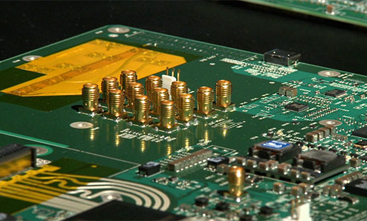
Double-sided Ball Grid Array (BGA) assembly maximizes component density without increasing board size, enabling high-performance designs for applications ranging from smartphones and IoT devices to medical and industrial electronics.
PCB School
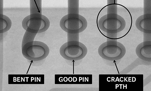
Managing strain during press-fit connector insertion is essential for high-density PCB reliability. Discover best practices and how San Francisco Circuits ensures reliable assembly for HDI, mil-spec, and medical applications.

PCB School
San Francisco Circuits covers the 8 types of PCB vias including blind, buried, microvias, through-hole, stacked, & thermal vias - what they are, how they work, & where they’re used in advanced PCB design.
PCB School
Discover why NIST 800-171 compliance is essential for PCB manufacturers. As a PCB buyer, learn how this cybersecurity framework safeguards your sensitive data & ensure you are engaged with a boardhouse that meets these requirements.
PCB School
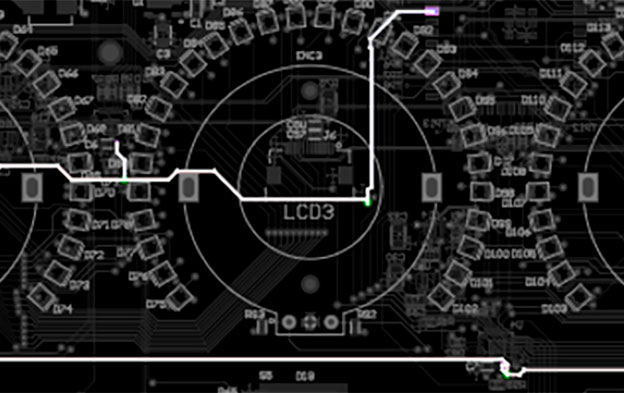
San Francisco Circuits covers board-level tips for the design & layout of high-speed circuits in advanced applications.
PCB School
PCB line tracing relates to both function and safety in circuitry. We discuss the significance of careful line tracing through both clearance and creepage.
